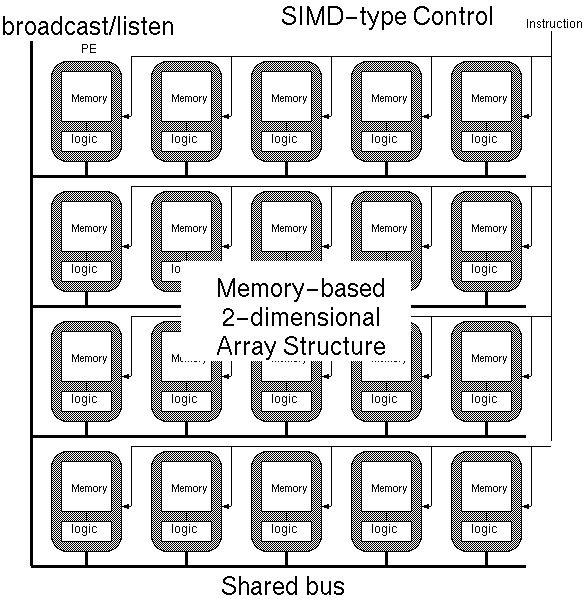
Functional Memory Type Parallel Processor: FMPP

The Functional Memory Type Parallel Processor (FMPP) is a memory-based
SIMD share-bus parallel processor which can enjoy some direct benefit
from memory VLSI technology. The FMPP architecture is schematized as
follows
 List of my papers is here.
The features of FMPP are summarized as follows.
- Memory-Based Simple Structure.
-
The FMPP has a memory-based simple
two-dimensional array structure like an LSI memory. Each processor contains
a bit, a word, or a group of words. We can obtain a very large parallel
computation space by the FMPP. A multi-chip construction is easily
implemented as same as for an LSI memory. The memory-based structure
enables a word of the FMPP to be accessed same as a conventional memory. I/O
pins are required for address, data and control. The number of data and
control pins is constant at any number of PEs, while the number of address
pins is proportional to the log to the base 2 of the number of
processors. Thus, total number of IO pins slowly increases as the number of
PEs.
- SIMD control method.
- All the PE of the FMPP are controled by a single
instruction. It is an SIMD (Single Instruction Multiple Data stream)
machine, where all processors work simultaneously by a single broadcast
instruction. The silicon area required by control logics is slightly smaller
than MIMD approaches.
- Simple communication network through a shared bus.
- The shared-bus is most simple way to connect multiple PEs. It
enhances the layout density, while applications on the FMPP should
remove inter-processor communication and reduce communication between
processors. An outer control logic or CPU can access the content of
each word on the FMPP through read/write operations word by word like
a conventional memory.
- Massively parallel computing on huge number of processors.
-
Memory-based simple structure realizes massively parallel computing. The
number of processors can be increased year by year as progress of memory
VLSI technology.
- Easy to achieve highly dense layout.
- Processors of today contain too
complex circuits and networks. Now, they are semi-automatically implemented
by logic and layout synthesizers paying the cost of silicon area. The
two-dimensional regular array structure and simple communication network of
the FMPP allows highly dense layout. All we have to do is to design a layout
pattern of a PE and to put it into array, which can be implemented by
interactive manual design strategies.
- Low power computing.
- Chandrakasan mentions that parallel processing
must decrease power dissipation. Suppose that two processors
work in parallel. The clock frequency of them may be half of that of a
single processor if the same through-put rate is assumed. On that condition,
the supply voltage can be dropped. The power dissipation of such a
two-processor system is 0.36 of that of a single processor system. Thus, the
FMPP must decrease the power dissipation considerably. In the Von-Neumann
system, data transfer between processor and memory consumes large power. The
FMPP also reduces power to perform processing inside memory to decrease
communication between memory and a processor.
Bibliography
- My Ph.D. thesis
- My
Paper List (Including Japanese)
- Bibliography about FMPP(including
Japanese Character)
- Bibliography about Functional Memory
- Bibliography about Vector Quantization
- Bibliography about Processors
LSIs
- Bit-parallel Block-parallel FMPP (BPBP-FMPP)
- FMPP for vector quantization
Slides
- slides for FMPP (frame)
Links
- Berkleey IRAM Project
kobayasi@kuee.kyoto-u.ac.jp
Last modified: Thu Aug 26 09:59:07 JST 2021